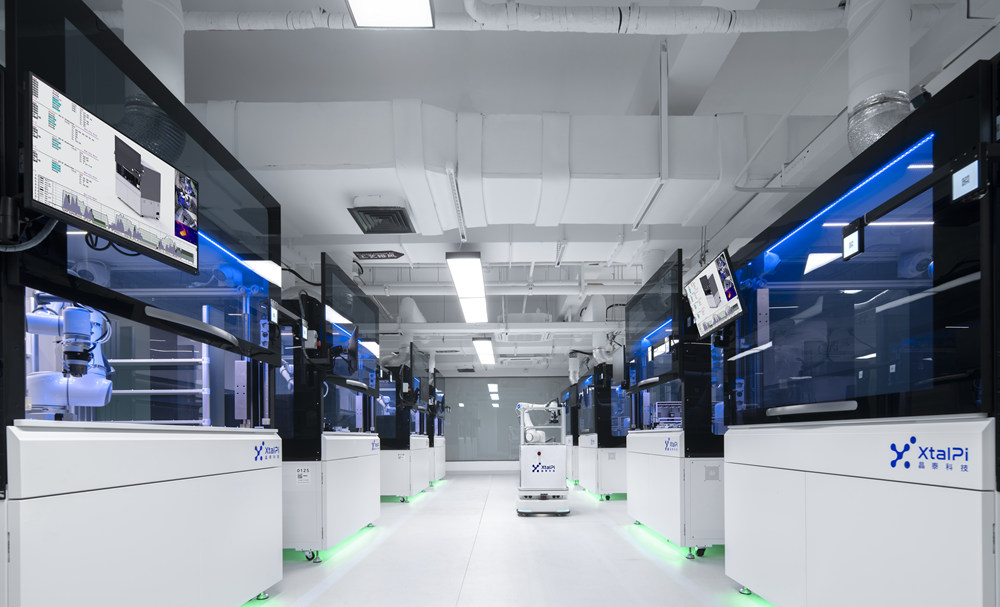
The new technology shortens the preparation cycle to 1.5 days.
Recently, I was fortunate enough to witness a major breakthrough in China’s scientific research community: the Clean Energy Materials and Devices Team of East China University of Science and Technology successfully developed a universal growth technology for perovskite single crystal wafers. The emergence of this technology not only significantly shortened the crystal growth cycle from the traditional 7 days to 1.5 days, but also realized the low-temperature, rapid and controllable preparation of more than 30 kinds of metal halide perovskite semiconductors, laying the foundation for a new generation of high-performance optoelectronics. The device provides a rich selection of materials.
This breakthrough by Chinese scientists in the field of crystal growth has undoubtedly attracted widespread attention around the world. As a new semiconductor material with excellent photoelectric properties and solution-preparable properties, metal halide perovskite has shown great application potential in the fields of solar cells, light-emitting diodes, and radiation detection. However, the preparation of perovskite single crystal wafers has long been a bottleneck restricting its practical application.
Traditional preparation methods have problems such as long growth cycles, high temperatures, and limited types, making it difficult to meet the material needs of high-performance optoelectronic devices. However, through in-depth experimental exploration and theoretical simulation, the team from East China University of Science and Technology successfully revealed the key role of the mass transfer process in crystal growth and developed this revolutionary universal crystal growth technology.
It is understood that this technology uses a growth system represented by dimethoxyethanol to significantly increase the diffusion coefficient of solutes by finely regulating the dynamic process of micelles, thereby achieving a substantial increase in the crystal growth rate. This innovative technology not only reduces the growth temperature, but also improves the quality of the crystal, opening up a new path for the preparation of perovskite single crystal wafers.
The world is witnessing this technology in action. In the laboratory of East China University of Science and Technology, researchers demonstrated centimeter-scale single crystal wafers prepared using this technology. These wafers are not only large in size and high in quality, but also have a greatly shortened growth cycle, providing strong material support for the research and development of optoelectronic devices.
In addition, the team also used this technology to assemble high-performance single-crystal wafer radiation detection devices, demonstrating its advantages in self-powered imaging of complex objects. This device can achieve high-quality imaging under low radiation intensity, which is of great significance for reducing the harm of medical radiation to the human body.
This breakthrough not only won Chinese scientists an international reputation in the field of crystal growth, but also brought new hope to the development of global optoelectronic devices. As a foreign journalist, I deeply feel China’s strong strength and enterprising spirit in technological innovation.
In the future, we look forward to the Chinese scientific research team continuing to make more breakthroughs in the field of crystal growth and contributing more to global scientific and technological progress. At the same time, the promotion and application of this technology will inject new impetus into the sustainable development of human society.


